ANSYS® model, the partial 1D ANSYS® model and the MHD-Valdis model are
presented respectively in Figures 10, 11 and 12.
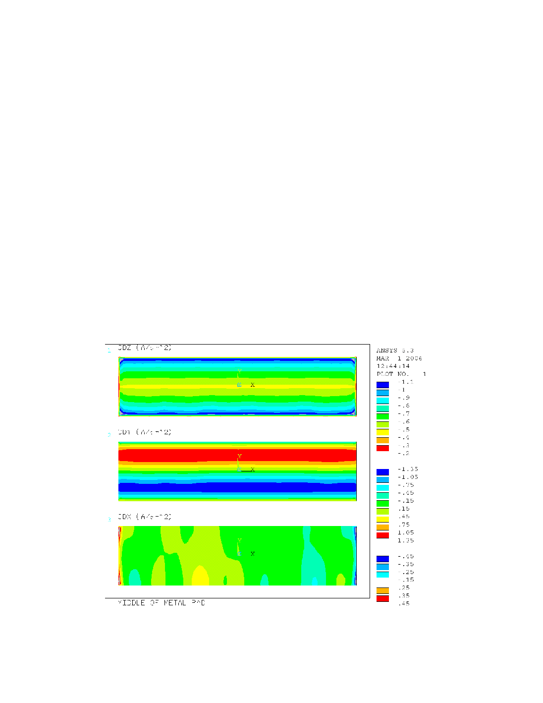
The impact of increasing the ledge toe thickness from 4 cm to 10 cm is a bit less
the cathode surface creates a local perturbation close to the ledge toe position. That local
perturbation is more or less well captured depending on the accuracy of the geometry
representation in the model. On the global scale, all three models correctly predict a
slight reduction of the intensity of the lateral horizontal current density (Jy) field. As the
collectors bars are rodded up to the edge of the cathode blocks, up to a certain point
having more ledge toe thickness can be a good thing. Only carrying up the cell stability
analysis will indicate if the cell will be more or less stable after this change of ledge toe
thickness.
It would have been interesting to analyze the impact of having even more ledge
preventing us to run the model with more ledge toe thickness.