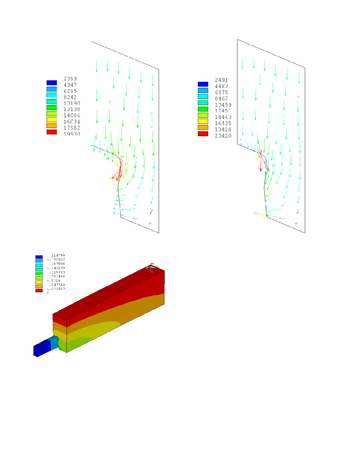
close of being equal. But is the current density in the cathode
block edge very different now? In order to answer that question,
one only has to compare Figure 5 with Figure 7 presenting the
current density solution obtained while using the temperature and
pressure contact resistance property in the model.
interface section. Now at least that tool can be used to investigate
how to improve the situation.
calibration it is reproducing "measured" data. Yet, before starting
to use the model as a design tool, it is also a good idea to test the
model mesh sensitivity. The initial model is using a mesh that is
much finer that the one of a standard TE cathode side slice model.
But is the mesh fine enough to well represent the contact behavior?
mesh has 2592 3D solid elements and 1065 2D contact elements. It
took only 566 seconds to solve on a 64 bits dual core Intel Centrino
T 9300 Cell Precision M6300 portable computer running ANSYS®
2760 2D contact elements. Solving the same problem with that
refined mesh took 5225 seconds, so about ten times more than
solving for the initial mesh.
the accuracy of the solution is concerned the initial mesh is clearly
good enough. But the current density vectors presented in Figure 8
indicate that the finer mesh is helping a lot in the interpretation of
the results. In Figure 8, the current is concentrating itself in three
points where the contact pressure is concentrated.